The
Processor that we all know and use today is relatively young, all things considered. The first general purpose CPU, the Intel 4004, entered the consumer market back in 1971 which marked the start for home computers. Since then, the progress in processor technology has been astronomical and has been following
Moore's Law up to this day. However, the engineers at Intel and Motorolla didn't invent the modern CPU out of thin air. Let's have a look through history to see how and where it all began, how it has progressed, where we are at right now, and speculate what we can expect for the future!
01001100 01100101 01110100 00100111 01110011 00100000 01100101 01111000 01110000 01101100 01101111 01110010 01100101 00100000 01110100 01101000 01100101 00100000 01010000 01110010 01101111 01100011 01100101 01110011 01110011 01101111 01110010 01110011 00100000 01100110 01100001 01101101 01101111 01110101 01110011 00100000 01100110 01101111 01110010 01101101 01110011 00100000 01110100 01101000 01110010 01101111 01110101 01100111 01101000 00100000 01110100 01101001 01101101 01100101 00100001
Let's explore the
Processors famous forms through time!
Let's explore the Processors famous forms through time!
Vacuum Tubes
Classic_shot_of_the_ENIAC.jpg
Eniac_Aberdeen.jpg
ENIAC_Penn1.jpg
Two pieces of ENIAC currently on display in the Moore School of Engineering and Applied Science, in room 100 of the Moore building. Photo courtesy of the curator, released under GNU license along with 3 other images in an email to me.
Copyright 2005 Paul W Shaffer, University of Pennsylvania.
On the left is a function table (for reading in a table of data). There are four panels, the left-most one controls the interface to the function table. The third one is an accumulator - memory for storing a 10-digit number, which can be added into.
Glen_Beck_and_Betty_Snyder_program_the_ENIAC_in_building_328_at_the_Ballistic_Research_Laboratory.jpg
Reprogramming_ENIAC.png
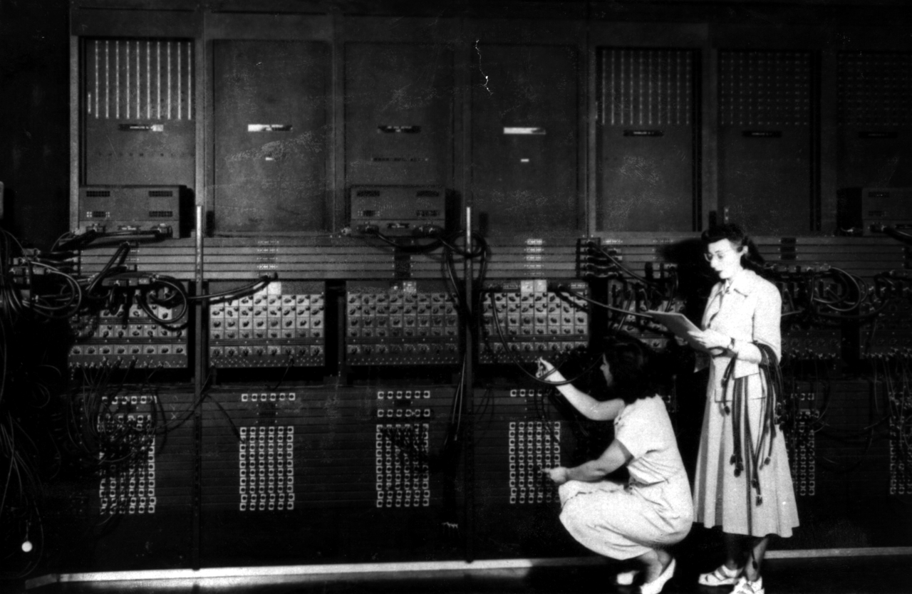
Two_women_operating_ENIAC_(full_resolution).jpg
Two of the ENIAC programmers, are preparing the computer for Demonstration Day in February 1946
World's_First_Computer,_the_Electronic_Numerical_Integrator_and_Calculator_(ENIAC).gif
Before the invention of
transistors in 1947, the first computer had already made its appearance. The Electronic Numerical Integrator and Computer, or simply ENIAC, was the first general purpose computer. The University of Pennsylvania, specifically its Moore School of Electrical Engineering, completed the build in December 1945 just after World War II had finished. Its purpose: making calculations and solving complex numerical problems.
The ENIAC relied on a massive list of components to perform its calculations, the most important one being the
18.000 vacuum tubes which performed the switching task that transistors do nowadays. However, these tubes would burn out fairly often, making them less reliable. The majority of the failures happened when the tubes were warming up or cooling down, the moment when they were under the most thermal stress.
We had a tube fail about every two days and we could locate the problem within 15 minutes.
The ENIAC was a big unit! The panels alone took up a space of 9m (30ft) by 15m (50ft). That's two average school classrooms combined!
Extra Info about the ENIAC
The ENIAC was an
enormous unit. It consisted of 40 panels each 60cm (2ft) wide arranged in a U-shape. These panels had different tasks within the computer. Some were accumulators, they would store the data between the different arithmetic operations such as addition (+), subtraction (-), multiply (x), division (/), and square rooting (√). While the accumulators stored the data, they couldn’t do so without the 6.000 switches and cables on the function tables. Others were panels performed other specific operations within the computer.
The University of Pennsylvania still has a few of these panels and parts on display in Moore School of Electrical Engineering. These include the Cycling Unit, the Master Programmer Unit, a Function Table, an Accumulator, and Digit Trays. They also have the later added Punch Card Reader, a Card Puncher, and a Card Printer to make programming the ENIAC a little bit easier.
In all, this computer required a lot of components. Aside from the 18.000 vacuum tubes present in the system, the circuit boards included 70.000 resistors and 10.000 capacitors. These were all soldered on the boards by hand along with other electrical components. This is 500.000 hand soldered joints just in one big system. To provide power to run the Electronic Numerical Integrator and Computer, it had its own dedicated power lines. The computer required 150 kilowatts of electricity to run continuously, which was a fair lot at the time.
Still, even with the relatively high power consumption and maintenance, it was worth every cent. Compared to a hand calculator, the ENIAC was capable of performing math at an insane speed for its time. For example, a ballistics calculation would take 12 hours with a hand calculator, but that same calculation took just 30 seconds with the computer. It was faster by a factor 1440 and the results would be less prone to (human) errors.
If you want to read even more about the ENIAC, the Smithsonian Library has a
Report on the ENIAC available to read.
The first programmers of the ENIAC were a group of six women. In order to make sure the computer would be programmed correctly, they first had to figure out the program on paper. Then the program had to be mapped to the ENIAC itself, which could take weeks, by manipulating a multitude of switches and cable plugs. If you fancy programming, definitely give
this online tutorial a look. It shows how to implement a modulo function on an ENIAC simulator which should give an impression of what a program on this computer would look like.
Learn more about Computers using Vacuum Tubes
The ENIAC was one of the first computers, but it had its flaws. With the war going on, there was a freeze on the design in 1943. The result was a lack of innovation for this historic computer. The most important feature missing on the ENIAC was the ability to store a program on a computer. Nowadays, a computer stores all its programs on its harddisk, but that was not the case back then.
Von Neumann Architecture
Still, even with the freeze in place, the original designers of the ENIAC,
John W. Mauchly and
J. Presper Eckert, didn’t sit quietly and instead worked on a new design which would be simpler and more powerful. At the time,
John von Neumann was consulting Moore School on this new computer design, which would later be called the Electronic Discrete Variable Automatic Computer or EDVAC.
During his time as a consultant, Von Neumann attended many meetings at which the concept of stored programs was elaborated. At these meetings, he made many notes describing the ideas developed in these meetings in a formal logical language. On his commute by train, Von Neumann wrote an entire report by hand which he sent back to the university. The administrator and security officer of the ENIAC, Herman Goldstine, had the report typed, duplicated, and distributed to the US government and educational institutions worldwide. The
First Draft of a Report on the EDVAC caused a widespread interest in this new technique which would lead to a new generation of computers.
Based on this report, a new computer architecture evolved promptly named the
Von Neumann Architecture. It was the first one to define a way to build stored-program computers. Many educational and government institutions created new systems based on this revolutionary architecture. A few notable ones were the EDVAC at the University of Pennsylvania, the Electronic Delay Storage Automatic Calculator (EDSAC) at Cambridge University, and the Ordnance Discrete Variable Automatic Computer (ORDVAC) at the University of Illinois.
All these new systems still used vacuum tubes as their main component to control the electrical circuits. However, many processors nowadays still use the same hardware mechanism to encode and store both data and program instructions. So, at its core, the Von Neumann Architecture is still used to this day in modern processors.
EDVAC
The Electronic Discrete Variable Automatic Computer was the first built using the new Von Neumann Architecture. After finishing the design, the government signed a construction contract in April 1946 therefore ordering the build of the system. Ultimately, in 1949 the EDVAC was delivered to the Ballistic Research Laboratory. It became the first binary serial computer, capable of addition, subtraction, multiplication, division with a memory capacity of 1.024 44-bit words. In modern day terms, that is equal to 5.6 kilobytes, roughly the size of a small text file.
The EDVAC was much smaller, yet already stronger, than the ENIAC. With almost 6.000 vacuum tubes and 12.000 diodes, it consumed just 56 kilowatts of power. That is almost one third of what the ENIAC had in components and power consumption. Not only that, it also used less space with just 45m2 (485ft2) and weighing in at almost 8 tons. Furthermore, the EDVAC was capable of using floating-point arithmetic since receiving a few upgrades in 1958, which means it could calculate things as 2.2 * 3.25. Before, only full integers could be used in the calculations.
In the end, the EDVAC ran from 1949 until 1962 when it was retired and replaced by the
Ballistic Research Laboratories Electronic Scientific Computer.
EDSAC
The Electronic Delay Storige Automatic Calculator was an early computer made by Cambridge University and was heavily inspired by the First Draft of a Report on the EDVAC.
Maurice Wilkes and his team started the construction of the EDSAC in 1947 and finished it early 1949 with its first program running on May 6th 1949. It used a different technique to store data in memory; instead of vacuum tubes, they opted for mercury delay lines. For the logic, they still used the vacuum tubes. By drastically reducing the amount of vacuum tubes, they were able to cut the power consumption back to only 11 kilowatts of electricity.
In the end, the EDSAC ran from 1949 until 1958 when it was superseded by the EDSAC 2. Unlike the ENIAC and EDVAC, the Electronic Delay Storage Automatic Calculator was primarily used in university research supporting the Cambridge University Mathematical Laboratory. This system has played a pivotal role in the research of many renowned scientists. It helped at least three Nobel Prize winners, John Kindred and Max Perutz (Chemistry, 1962), Andrew Huxley (Medicine, 1963), and Martin Ryle (Physics, 1974) who all acknowledged the role that the EDSACs computing power had played in their research.
Currently, there is a project going on at the National Museum of Computing to replicate the original EDSAC. If you love a bit of history, and you live in the UK, it is definitely worth a look! If you don't live in the UK, don't worry, the museum has
a webpage set up to get more information on the project and its current state.
From Printed Circuit Boards
To Integraded Circuits
With vacuum tube computers already in use by major universities and government instances, the demand for these mathematical geniuses for the consumer market rose drastically. However, the cost of maintenance and tubes could not realistically be covered by most private individuals or even commercial companies. That is even without taking the sheer size of these computers into consideration. Fortunately, during the 50s, a new type of computer came into the playing field which enabled smaller to mid-sized companies to purchase computing power. Two decades later, a new advancement in processor technology would pave the path for home computing that we all know, love, and use today. At the center of these advancements is the transistor, invented in 1947. This quicker and more power efficient component would dominate the processor industry for years to come.
Transistors on a Printed Circuit Board
Around the mid 50s, two major companies developed the next generation of computers by replacing the vacuum tubes for transistors. They created modules; printed circuit boards with transistors, resistors, capacitors and other electronic components soldered directly onto them. Each type of module had a specific feature or role within the computer. A system would be made up of these modules and such a system could easily be expanded in functionality, memory, or processing capacity by adding more modules. One of the companies, IBM, even created the IBM Standard Modular System which remained in use with legacy systems well throughout the 70s after the introduction of the IBM 1401 in 1959.
Digital Equipment Corporation was a fierce competitor of IBM at the time. They introduced their first fully transistorised computer, the Programmed Data Processor-1 (or PDP-1), in 1959. This machine became pivotal in computer history. Many applications that we deem the norm today were first created on or for this system. The PDP-1 is the original hardware for:
Playing the first video game, Spacewar!;
The first text editor;
The first word processor
The first interactive debugger to help programmers find the defects in their code;
The first credible computer chess program;
And many more.
The PDP-1 also caused a big shift in philosophy of computer design: it was the first commercial computer that focused on the user interaction, rather than just the computing efficiency.
The PDP-1, the IBM 7070, and their successors were very popular among companies. These systems were much smaller than the vacuum tube computers available and more maintenance friendly. However, do not be mistaken, these systems were still large, taking up the space of two refrigerators with ease and weighing up to a metric ton. In hindsight, it is a bit ironic that companies called them minicomputers at the time. However, it did fit their initial description: they were smaller general purpose computers and they were sold at a lower price than a full
mainframe, which was still the size of the ENIAC or EDVAC during those days.
The PDP-1 is famous for being the most important computer that created the hacker culture at MIT. The first reference to malicious hacking came from MITs student newspaper, The Tech, talking about "telephone hackers". Apparently, a few student hackers from MIT were tying up the lines with Harvard, configuring the PDP-1 to make free calls, and accumulating large phone bills.
Transistors in an Integrated Circuit
During the continued the development of more minicomputers, a shift in electronic circuit technology happened. Since the late 50s, around the time when the first transistor computer came to market, pioneers like
Robert Noyce at
Fairchild Semiconductor were experimenting with a new way of creating an electronic circuit; one so tiny, that they cannot be seen by the naked eye. This new technology would be the breakthrough to make computers more affordable and smaller, and, overtime, to our wrists and pockets. Integrated circuits brought a new era of computing technology to us.
So, what is an integrated circuit? The science and technology behind this is very complex, but here is an attempt at a simplified explanation. Integrated circuits are like teeny tiny cities with buildings and roads made in silicon. These buildings could be transistors, resistors, and capacitors with little roads interconnecting them. Lightning travels between and through the buildings, resulting in a miniature full electrical circuit. Essentially, it is the same as the printed circuit boards with the electronic components soldered onto them, but much much much smaller.
Nowadays, we cannot live without this technology. The majority of electronics that we use today have these integrated circuits. It doesn't only apply to processors, it is used for a wide variety of components. Do you play video games using a graphics card? Yep, that has ICs in them. Saving pictures and files to your SSD? You bet that's made of ICs. Cameras, whether on your phone or as a camerabody, also littered with ICs.
Maybe, one day, I will attempt to explain in much more detail how integrated circuits and the technology behind it to make them work. For now, just know that it is a miniature electrical circuit. However, if you want to learn more about it, and don't want to wait for me to tell you, I have a few resources that you might find interesting. The materials are complex, just so you know what you're getting into. Learn more about integraded circuits, the metal-oxide-semiconductor field-effect transistor, the applications of MOSFET in the integrated circuit industry, and ASMLs role in the semiconductor industry.
A Timeline of Microprocessors
Since the introduction of the first general purpose microprocessor in 1971 by Integrated Electronics (aka, Intel), processor technology has advanced at a rapid rate.
Gordon Moore, one of the founders of Intel, speculated that processors would double their transistor count by every two to three years, increasing in speed and operating capacity with each cycle. This observator was later named after him:
Moore's Law. Processor technology hasn't disappointed, and still is mostly adhering to this observation. Hence, to keep track of the microprocessors from history, this timeline highlights the most popular CPUs of the past 50 years.
4-bit
The Intel 4004 is generally considered the first general purpose processor that gave rise to the integrated circuit technology. With an astounding 2300 transistors fitted into a 12mm
2 die, roughly the head of a small nail, having a computer at home suddenly became a possibility. The chip was fairly small and still powerful enough to cater to the users needs of that time. While it wasn't used much in the personal computer sphere, it did show the potential that integrated circuits would provide to make this a reality.The Intel 4040 was released three years later as an improvement upon the Intel 4004. Both these chips were designed by the same person,
Federico Faggin, who would design a few more impressive CPUs in the oncoming years.
What was your first Processor or Computer? Let me know in the comments!
8-bit
Not long after the release of the Intel 4004, the Intel 8008 took the stage as the first consumer grade 8-bit CPU. Originally, this processor was not intended to be released as a stand alone CPU for the market.
Computer Terminals Corporation commissioned Intel to create a CPU for their
Datapoint 2200, because they didn't have the capacity to design and manufacture processors themselves. However, since the processor didn't meet the requirements, CTC allowed Intel to use the design for themselves. After rebranding it, Intel released the Intel 8008 in 1972. The performance of the chip was dreadful, but it was the first 8-bit processor nonetheless.
The Origin Story of the Intel 8008, the first commercial 8-Bit processor.
The Seed of the Personal Computer
In 1968, Computer Terminals Corporation (later named, Datapoint) made its entry into the computer world. They wanted to bring a more advanced terminal system to the smaller companies and even the homes of people, so they could experience the power of the computer. With three prototypes of the
Datapoint 3300, they took the market by storm to the point where they had to use other manufacturers, even one that made motorcycle helmets, to get the production of these systems flowing consistently.
A year later, CTC wanted to improve upon their design. The founders, Jon Phil Ray and Gus Roche, envisioned an even more intelligent terminal system. Two of their employees started working on a new instruction set architecture for a new processor for the new Datapoint 2200. However, CTC didn't have the capacity to come up with a CPU design that would fit the developed architecture. Since they were already using the chips from Intel and Texas Instruments for their previous computer, the most logical step would be to go to these companies.
Creative Business Practices
However, the company didn't have a lot of money on hand. In fact, they had outstanding invoices with the two chipmaking giants. Fortunately, that didn't deter Ray and Roche from coming up with an interesting gamble. The two arranged a dinner with the president of Intel,
Robert Noyce, and the president of Texas Instruments. Before this meeting, Ray drew the schematics for a microprocessor and the new instruction set architecture on two postcards and during the dinner he gave one to each president with a bet: the company who first can create a computer on one chip would forgive CTCs outstanding debts.
But why should the winner of the bet forgive these debts? CTC had bought, and still would need, a lot of chips and components from these tech giants. Without the funds to pay for it all, they had racked up some serious debt. So, CTC wasn't just looking for a way to source a new computer, they were also looking for a way to cut costs. The idea here was that the company would do business with the winner — meaning that whichever company could produce the chip, would also be the one selling these chips to CTC. Ray and Roche believed that this would be the future of computers and that there was a huge market for this type of system, which would bring a lot of profit to the winner as well.
Initially, Noyce questioned this approach. At the time, Intel was selling a lot of computer components; putting all the components in one processor would surely reduce sales and therefore Intel would undoubtedly lose money on it. Not entirely a wrong assumption for that time, but we all know how it turned out in the end. Still, both companies agreed to the bet and got to work.
Texas Instruments was the first to back out of the bet. By late 1970 or early 1971, they couldn't deliver a stable and reliable processor. By this time, Intel still had not produced a demo product, so CTC decided to go down the transistor computer route instead which they could do themselves. This is the reason why the Intel 8008 instruction set was first used on a transistor computer, rather than a microprocessor for the first year of its existence.
Rebranding a "Failed" Product
By the end of 1971, Intel managed to come up with a processor that was capable of running the code. However, CTC decided not to go through with the CPU they had made. In the demonstration, the CTC 1201 as this processor was called at the time did not meet the performance requirements of CTC management. Furthermore, it needed a lot of extra accessory chips to make it work, and they wouldn't be able to meet the release dat for the new Datapoint 2200.
However, CTC had effectively contracted Intel to make the chip design and to produce it. So, to avoid paying the costs of the commission, they released Intel from their contract allowing them to use the CPU design to make a product themselves. Within a few months, Intel had rebranded the processor to the Intel 8008 and marketed it as the first 8-bit CPU of its time.
Noyce's concerns at the time were absolutely valid. No one could ever have predicted how popular the successors of the Intel 8008 would become. For all they knew, they would lose a lot of business with fewer chips needed in computers. Fortunately for Intel, they become the leading company in the advancement of processor technology which definitely has contributed to their solid position in the CPU market to this day.
From this point forwards, the competition within the processor manufacturing and designing sphere was fierce. New companies would spring up, designs would be used and improved; the same designers sometimes would switch company, or start up their own. Prime examples are people like Federico Faggin and the engineers at Motorola.
Faggin had improved the design of the Intel 8008 massively, bringing the Intel 8080 to the world in 1974. Aside from the improved performance, this processor required fewer support chips in order to run properly in a system. Just after releasing the Intel 8080, Faggin decided to start a new company,
Zilog, dedicated to manufacturing microprocessors. After two years, in 1976, he released the Zilog Z80, a processor with an improved design of the Intel 8080, and fully compatible with it as well. The company even made fun of the Intel 8080 in a 2-page advertisement in a magazine. The Zilog Z80 was a hugely successful processor, partially because of its improvements upon the Intel 8080, and partially because it was much cheaper.
Motorola released their first 8-bit processor in 1974 as well, the 6800. However, things weren't all rainbows and sunshine there either. Motorola's Semiconductor Products Division management was overwhelmed with problems showing no interest in business proposals given by their processor engineers. This ultimately lead to a few of them walking off to create
MOS Technology. Within a year, MOS Technology released a new processor that, like the Zilog Z80, was much cheaper than its predecessor: the MOS 6502.
The introduction of the Zilog Z80 and the MOS 6502 singlehandedly brought us the home computer revolution in the early 80s. Suddenly, it was possible to have a computer at home for a reasonable price which lead to an enormous boom. The VIC-20 used the MOS 6502 chip, the Apple I & II also featured the MOS 6502; the famous Commodore64 used its improved version, the MOS 6510. Sinclair's ZX81 shipped with the Zilog Z80, making it possible to own a computer for just $99 (equivalent to roughly $320 in 2022 and the Sinclair ZX Spectrum featured the improved Zilog Z80A. However, not only home computers benefitted from the 8-bit CPU. Many of the first gaming consoles started out with these CPUs. The Nintendo NES had a clone of the MOS 6502; the Atari 2600 featured the MOS 6507; and the Sega Master System used the Zilog Z80a.
Did you know that the WDC 65C02 by Western Design Center is still in active use to this day? This little 8-bit CPU (and its bigger 16-bit brother, the WDC 65C816) protect the lives of many people with embedded heart defibrillation and pacing systems! They consume a small amount of power and are very stable, making them the perfect candidates for healthcare applications. Not only that, many hobbyists love toying with these chips! Just like our writer here, who wants to Build a Computer From Scratch.
The 8-bit processors have laid a foundation in the computer industry that no other CPU can match to this day. They have started the revolution which gave us the home computer, the gaming console which ultimately has lead to the advancement of the technology as a whole. Without these chunky CPUs, we never would have had smart watches or smartphones. These devices are much faster and smarter than our 8-bit friends, but they wouldn't have existed without them.
Want to learn even more about 8-bit CPUs and Computers?
I see you want to learn more about 8-bit CPUs and Computers, that's awesome! I have accumulated some resources for you. Some are reading materials, others are YouTube channels that cover this type of information and projects. Have a look!
Microprocessor (Wikipedia); this covers all of microprocessors, not just 8-bit, but still as interesting!
Microprocessor Chronology (Wikipedia); this is an extensive list of all the microprocessors created to this day (or roughly..).
The 8 Bit Guy; an awesome YouTuber covering just about everything there is about old hardware.
Adrians Digital Basement; another awesome YouTuber covering old hardware.
There is probably a great many more resources, but this should get you started at least.
- ShadowPhoenix, the Writer
16-bit
The first 16-bit CPU was not a single unit; with the first 8-bit CPU released the year prior and the first 4-bit CPU two years prior, the design and technology capabilities to make a 16-bit single chip processor wasn't there yet. Instead,
National Semiconductor first opted to create a multi-chip 16-bit processor: the IMP-16 released early in 1973. It consisted of two primary components. The first was one chip called the CROM which stands for Control and ROM; it contained the
Control Unit to make sure that the processor performs the instructions in the right order and it had a chunk of Read-Only Memory for storing microcode coming from outside the CPU.
Four identical chips called the RALU comprised the second primary component; these chips had 4-bit Registers for storing the input and output of the
ALU which did all the calculations based on the instructions it was given from the CROM chip. These four chips worked in parallel to produce a 16-bit output and thus a 16-bit processor.
Almost two years later, in late 1974, National Semiconductor managed to improve on their IMP-16 design and produced the first single chip 16-bit processor; the National Semiconductor Processing and Control Element, or PACE. Soon, other companies followed with their first 16-bit single chip processors. In 1976, Texas Instruments introduced their TMS 9900 which was compatible with their TI-990 line of minicomputers, competing with other companies, like
DECs PDP series, which were transitioning from transistor computers to using microprocessors during this time.
Intel x86
In 1978, Intel released their, now infamous, Intel 8086. This processor marks the start of the
Intel x86 series which powers most modern personal computers to this day. The Intel 8086 used the same microarchitecture as its 8-bit predecessors. This meant that programs written for the Intel 8008, 8080, and
8085 (1977) could run perfectly on the Intel 8086 without altering the code. It was the first case of backwards compatibility in computers. A year later, the Intel 8088 was released and became hugely popular because it was the CPU of choice for one of the very first personal computers: the IBM PC. With their subsequent releases of the 80186, 80188, 80286, and the 80386, their first 32-bit CPU, Intel became the most dominant CPU player in the PC market with the processor family's backwards compatibility.
Did you know, the first computer of Dimitris, the founder of WorldAnvil, featured the Intel 80286? Its standard clock was 6MHz and had a turbo up to 12MHz, which was really fast for its time. To give an idea how fast computers are nowadays, the Intel Core i5-13400 (an average Intel Core i5) runs natively on 3.3GHz, which is 500x faster than the 80286s standard clock, and has a turbo up to 4.6GHz. The 80286 had 120.000 transistors, whereas the i5-13400 has 14200 million transistors, that's over 100.000 times more transistors!
The x86 processors were a great hit with the standard use of computers at the time. Most people were doing simple things on computers at the time; think about writing, programming small programs to automate things for them, playing and making relatively simple games using programming languages such as BASIC and Pascal. For standard use, the x86 processor family was perfect, but there was still a gap in the advanced user market, specifically those that perform a lot of complex mathematical computations.
However, Intel played this game well. In order to keep their x86 family running as fast as possible for the average user, they did not include an extensive floating-point unit in the CPU design. Instead, they created a separate coprocessor that would speed up the floating-point arithmetic operations such as addition, subtraction, multiplications, division, and square root. It also added extra functionality, such as computing transcendental functions such as exponential, logarithmic, or trigonometric calculations. Thus they introduced the
x87 family, a series of coprocessors (the
Intel 8087, 80187, 80287, 80387) with the same backwards compatibility as the x86 series. For each x86 member (except the 80188), there was a corresponding x87 coprocessor with each combination forming a single multi-chip microprocessors. The two chips were programming as a unit, using a single integrated instruction set.
The people who needed the extra mathematical computing power, which were primarily universities and companies, could manually add the extra x87 coprocessor hardware to their systems drastically improving the computation times for more complex mathematical equations.
32-bit
Rise of Motorola
Shortly after 16-bit processors were available for consumers to purchase, the first 32-bit CPUs started to appear. One of the most prominent 32-bit processors came from
Motorola. Their 8-bit
M6800 was hugely popular at the time, but sales were already dimming especially with their fierce cheaper competitors (
Zilog Z80 and
MOS 6502 primarily) taking over a good chunk of the market. By 1976, Motorola was aware of Intel and Zilog working on a 16-bit CPU, the
Intel 8086 and the
Z8000 respectively. Instead of trying to compete with them directly in the 16-bit space, the company opted to aim directly for a 32-bit processor to get ahead in the game.
Early on in the development, Motorola abandoned the idea of backwards compatibility with the M6800; they felt that its 8-bit design would be too limiting for a new and innovative 32-bit processor. Their primary goal was winning back computer vendors, such as
Apple and
AT&T, by immensely improving the performance, aiming for a speed of
1 MIPS. Free from the 8-bit limitations, they presented the world with the Motorola
MC68000, otherwise known as the Motorola 68k or the m68k, in 1979.
They were competing directly against the
Intel 8088 in the
IBM PC. Their m68k powered many systems, such as the iconic
Apple Lisa and the
Apple Macintosh, the first two systems to run an operating system with a graphical user interface.
Starting the early 1990s, the use of the
m68k family in systems reduced as the
PowerPC family, another 32-bit CPU that was made in collaboration between IBM and Motorola, made its way into new iterations of Apple computers throughout the 90s.
Did you know that at one point there were more MC68020 processors in embedded equipment than Intel Pentiums in PCs?
The m68k was a good processor right out of the gate, but there certainly were improvements to be made. For starters, the
MC68010 added
virtual memory support, creating the illusion to users that they have a large chunk of main memory with some nifty tricks.
Next up was addressing the "32-bit" m68k. People considered the m68k 32-bit, because the CPU registers could hold 32-bit values. However, that didn't mean that all the CPU internals could hold data values of this size. The
data bus of the m68k was 16-bit, whereas its
address bus was 24-bit. The
MC68020 changed that, tranforming the processor with full 32-bit data and address busses.
The last few changes happened in the last interations of the CPU. First, the
MC68030 integrated a
memory management unit into the chip, removing the need for a separate MMU chip on the computer board. Later, the
MC68040 added a
floating point unit in the processor, which drastically improved the mathematics performance.
Intel and AMD; From Partnership to Competitors
In the meantime, Intel didn't sit still. While they were still primarily riding on the success of their 16-bit processors of the x86 family in the early 80s, they had started the development of a 32-bit version on the same instruction set architecture. Three years after the release of their latest 16-bit CPU, the Intel 80286 in 1982, the company introduced the
Intel 80386 which was later renamed to i386. It followed in the footsteps of the Intel 8088, powering many personal desktops and company workstations as well. The i386 was widely adopted, not just in personal computers, but also in embedded systems. The processor, or one of its many derivatives, are common in aerospace technology and electronic musical instruments, among others. Its successor, the
i486 from 1989, was the first processor to exceed the 1 million transistors in its CPU die mark.
Did you know that the i386s production was discontinued in 2007? This chip had been produced for over 20 years! The Linux Kernel supported this chip the longest, up until the very end of 2012.
Up until this point, Intel had a partnership with AMD and a few other companies, dating back to the early 80s. In order to seal the deal with IBM to put the Intel 8088 in their flagship personal computer, Intel had to accept one important condition; IBM wanted to make sure there was a second-source manufacturer capable of producing the processor. Back in those early days, it was a common practise to license other companies to manufacture and sell components originally designed by another company. This was done to make sure that there would always be someone capable of producing the necessary components, so a popular and profitable product can always be made even when the primary production facility burns down for example. Thus, AMD had the designs of the Intel microprocessors in their databases to be able to make them.
While the processor designs of the early x86 family were licensed, Intel decided not to do this for their new flagship line of CPUs: the
Intel Pentium. From 1993 until 2003, the
Intel Pentium series sealed the domination of Intel in the personal and business computing market. Ranging from personal desktops to the first laptops; from workstations to the first set of cell- and smartphones; nearly everyone was using Intel microprocessors. Over the course of these 10 years, their CPUs increased in complexity, which is determined by the amount of transistors, and capability, which is determined byt he amount of instructions a CPU can execute per second (aka MIPS), by at least three orders of magnitude.
Intel may have dominated the market during this time, but they still had good competition with IBM and Motorola with their PowerPC line that were powering many of Apple's machines. Furthermore, AMD also wasn't keeping quiet either. Even though they didn't have any licenses for the Intel Pentium series, they still had the previous x86 designs as a blueprint for their new designs. In 1991, just before the release of the Intel Pentium, AMD introduced a new CPU that was compatible with the i386, the
Am386, designed by their engineers. From this point, AMD became, and still is, a direct competitor of Intel, forcing the company to innovate and to create better microprocessors. The
AMD K5 (1996) and
AMD K6 (1997) were the predecessors that had lead the team towards the fastest processor for its time; the iconic Athlon line launched in June 1999 and was for two years the fastest x86 CPU breaking the 1GHz speedbarrier.
64-bit
During the early 1990s, a few companies were already experimenting with a 64-bit architecture for their CPUs. The majority of these companies focussed on delivering microprocessors for large servers and workstations in big companies.
Digital Equipment Corporation was one of the first to introduce the next generation of server CPUs; DEC unveiled the
Alpha 21064 to the world during the 39th International Solid-State Circuits Conferences in mid-February 1992. Five years later,
Sun (now known as
Oracle) launched the
UltraSPARC; and in 1997
IBM released their 64-bit processor, the
RS64. Only big corporates had access to purchase these products, since they were specifically designed for workstations and servers which often required significantly more computing power than normal consumers.
Aside from the
Nintendo 64, which was the first gaming console to feature a 64-bit CPU (hence the name), these advanced processors were not available to regular customers until much later. Roughly 10 years after DEC introduced the Alpha 21064, the AMD Athlon 64 entered the consumer market, bringing 64-bit microprocessors to the regular desktop. These CPUs were compatible with Intels x86 series, allowing them to run code made for all the previous x86 processors without any performance loss. Since it was capable of that, they called it the x86-64 architecture, or AMD64 architecture. Of course, Intel couldn't stay behind for long in this heated processor market if they wanted to maintain their leading position. Soon after, Intel followed with a near fully compatible
64-bit extension of their x86 instruction set architecture in the fourth generation of the Intel Pentium 4.
The shift to 64-bit microprocessors had an immense effect on the software landscape at the time; especially for
Operating Systems. Many of the early operating systems developed a 32-bit and 64-bit version, the latter always capable of running the 32-bit software without any performance issues, partially due to the x86 implementation. The 64-bit OS versions fully utilised the extra capabilities of these new CPUs, two of which stuck out the most and had the most impact. For starters, the registers were now expanded to contain 64-bit data values. Secondly, these new processors also had double the number of general purpose registers, allowing the operating system to store more values inside the processor to calculate things.
Imagine this: the CPU has a storage space with many shelves next to the calculator. It uses the shelves to store values: the inputs for the calculator and the output. These shelves can hold 32 bits of data. To give you an idea, with 32 bits, 32 zeros and ones, you can create 4,294,967,296 combinations of zeros and ones. These combinations form the letters we see on screens, the logic of things, just everything. You have decided to upgrade your CPU with a new and shiny one that is 64-bits. When you walk into the storage space, you see shelves that can hold 64 bits! 64 zeros and ones, which allow you to create 18,446,744,073,709,551,616 different combinations! Not only that, you even have twice as many shelves as before, meaning you cannot only store more on the shelves, but you also have more space to store other data! Think of all the new possibilities, the resources new programs can use now to do more advanced things!
The jump from 32-bit registers and internal busses to 64-bit certainly made the new generation of CPUs even faster than their predecessors. However, there is no such thing as having too much speed; the definition of "enough speed" different every day with consumers wanting even faster and more powerful desktops.
The development of software also shifted rapidly with these changes; programs are getting more complex and powerful, therefore requiring more and more resources to keep them running in a stable manner. This was especially apparent with the sharp rise of desktop gaming during that time with games requiring an enormous amount of space, relatively speaking.
To keep up with this demand on resources from programs and consumers alike, the first multi-core microprocessor designs were popping up during the mid 2000s and have been a staple in CPU technology since.
Essentially, there are two ways to provide a computer system with multiple processing cores. One way is by adding more processors to the system, this was often done on the motherboard directly by adding more slots to attach more CPUs to the system. This stacks the parallel processing power.
It doesn't increase the speed of the system, but it does provide more computing power. That is why this technique was, and still is, primarily used in high-end server equipment for companies who need to process tons of data every day. However, multi-socket systems require more and special hardware making them very expensive. The average motherboard only has one CPU slot, so special motherboards have been developed to provide and support two or four CPU sockets (the slot where the CPU goes). Furthermore, these systems need multiple processors. The prizes for these components easily skyrocket and aren't feasible for the majority of users.
The other option is much more user friendly and cheaper, too. The multi-socket system need multiple CPUs on one motherboard. However, the multi-core system puts multiple microprocessor cores into one processor which essentially achieves the same thing. For this option, the hardware of the day could be maintained. A motherboard still needed just one slot because there's still one CPU involved, and it was cheaper to produce this type of processor reducing the price drastically. Intel was the first to introduce a multi-core processor, the Intel Core Duo in 2007. This processor paved the path of multi-core CPUs making their way into the desktops of regular consumers. Soon after, AMD followed with the Athlon 64 X2.
Since the introduction of multi-core CPUs, AMD and Intel have been racing each other striving for better and faster processors. Both started out with a simple single core processor, and over time they have managed to contain up to 12 or even more physical cores. In more recent years, hyper threading has proved to improve the computing power of processors significantly, by creating two virtual cores in every physical core of the processor. In this race for the best CPU, Intel tends to focus more on achieving high frequencies of the CPU which gives them the leading position in the fastest single core performance. On the other side is AMD, whose processors stand vast at the top in multi-threaded performance, meaning they can do a lot of instructions in parallel.
Do you want to know more about the processor that powers your phone, smartwatch, and even washing machines?
Learn more about ARM processors here!
Every processor ever build has a custom processor architecture, one that is directly tied to the instructions that it should be able to perform. Many of the different CPUs during the 70s and 80s all had their own processor architecture, and ARM is one of them. Its origins stem from a small company with big ambitions after which the acronym was originally named: Acorn RISC Machine. Their goal was to create a very fast processor by utilising simple instructions to increase its speed, these instructions are also known as RISC. But what is ARM and RISC, and how do they tie into the world of processors?
RISC
As noted before, Intel has the x86 family, all originating from the
ISA created for the Intel 8086. The x86 ISA is a very large and complex architecture with many instructions at its disposal, which has its pros and cons. Having a wider variety of instructions, some of which consisting of multiple smaller instructions, means that programmers have to write relatively little code to make an Intel CPU execute a complex process. However, there is a price to be paid; big chunky instructions slow down the CPU. Furthermore, it also creates a fair bit of overhead as not all instructions necessarily have to be performed to get the same result.
On the opposite side of the instruction set architecture landscape stands
RISC, or Reduced Instruction Set Computer. As the name suggests, RISC opts to have less instructions available to the programmer, but every instruction is much simpler. The biggest con to this, is that the programmer has to write more code to make a RISC based CPU do the same thing as an Intel x86 based CPU. That being said, the simplicity of the instructions to make them faster to perform. Therefore, RISC hopes to offset the need to process more instructions with speed. The simplicity of the code, albeit longer but faster, makes RISC based CPUs the perfect candidate for embedded systems, and the most popular of all are ARM processors.
Acorn RISC Machine

The BBC Micro by StuartBrady, Public domain, via Wikimedia Commons Back in the early 80s, this small company
Acorn was looking around for inspiration for their next computer after their successful design of the
BBC Micro, considering to compete in this heated home computer market. The infamous Intel 8088 powered the IBM PC, and the Apple Lisa brought the graphics user interface concept to a wider audience, featuring the Motorola MC68000. However, these machines were not cheap. The Apple Lisa cost $9,995 (in today's money, that would be $30.000).
Engineers at Acorn studied all the CPU designs available, concluding that the existing 16-bit designs were "a bit crap"
source, since they offer only a slightly higher performance over than 8-bit BBC Micro design. Moreover, these 16-bit CPUs required a large number of support chips which drove up the costs, and their 32-bit cousins were even worse in that regard. The engineers were inspired by a series of reports from the University of California, Berkeley, showing the first designs for the RISC architecture. However, they were worried about creating their own CPU design since no one among them has ever done that. This worry was quickly settled after seeing a team of high school students making CPU designs on a set of Apple II computers. Thus they started their journey to build the Acorn RISC Machine.
Advanced RISC Machines
Over the years, many new versions of
ARM CPUs have taken a steady hold in the computing industry. They are quick and light, making them perfectly suitable for mobile applications. ARM licensed their CPU designs to other companies, such as Samsung, Apple, and many more. The majority of the phones runs on an ARM processor and very recently, they have emerged in more complex applications as well. Apple introduced their first fully ARM based processors in their flagship laptops in November 2020, with the third generation of Apple Silicon M3 chips released this year (2023).
The future of ARM is bright.
If you want to learn more about ARM and how it all started out, go and watch this YouTube video that has a very nice presentation about the introduction and the continuation of ARM.
Yesterday's Future is Tomorrow's History
So, what can we expect to change in the processor market in the future? It is hard to say what Research and Development departments at Intel and AMD are focussing on at the moment. From this point forward, it is a guessing game what will become the next big thing in processor space.
128-bit Processor
So far, CPUs have always doubled up in register size; from 4-bit all the way to 64-bit. It would seem logical that 128-bit CPUs are around the corner, and AMD happened to have released
their first 128-bit consumer CPU. That said, it is unlikely that these processors will become affordable for consumers anytime soon, since we hardly need more than 64-bit gives us.
Smaller.. and Smaller
Companies continue to strive for smaller transistors in order to fit more on a single processor die. The biggest player by far in this game is ASML, a Dutch company that builds the machines which can make these wafers consisting of many
CPU dies. Their newest generation of
EUV machines are expected to go to market in 2025, bringing 2nm technology to the fabrication of processors.
A 128-bit register provides us with an enormous amount of combinations... 39 numbers long... that's like writing 123,456,789 four times, and then adding another 123 at the end... that's... more than enough, don't you think?
A relatively obscure Dutch company
Artificial Intelligence
There are
rumours that hint towards more AI integration directly into the CPU hardware to optimise the execution of programs based on the users preference and usage. With many people and companies already using their processors for AI processing, it is only logical that processors more optimised for the use of AI will appear.
Change in Materials
Currently, wafers of silicon form the basis of the processor, where all the transistors and inner electrical pathways are etched. However,
new studies have found a different material to improve the speed of CPUs: Graphene. It can handle heat created by the electrical charge much better, potentially removing one of the processors biggest bottlenecks: overheating.
There is plenty still going on in the CPU space and hopefully many exciting things to come our way.
Our Writer looks up to the work done at ASML, if you couldn't tell that already. Maybe we can bully her into.. I mean ask her nicely to explain how lithography works, the process to make computer chips that powers all our electronic devices. That way she gets to learn even more about ASML and we get to learn more stuff too! Let our dear writer know in the comments!


.jpg")


.jpg")


Holy moly. What a beefy article. Thank you, ShadowPhoenix. Computer Adventures is one of the few settings I follow which makes me feel smarter with each entry.
Heh, yeah, there's a lot of information on processors. ^,^" I'm so glad you like the setting, hopefully you'll learn loads more things in the articles to come!